Counter installed: 12 January 2018
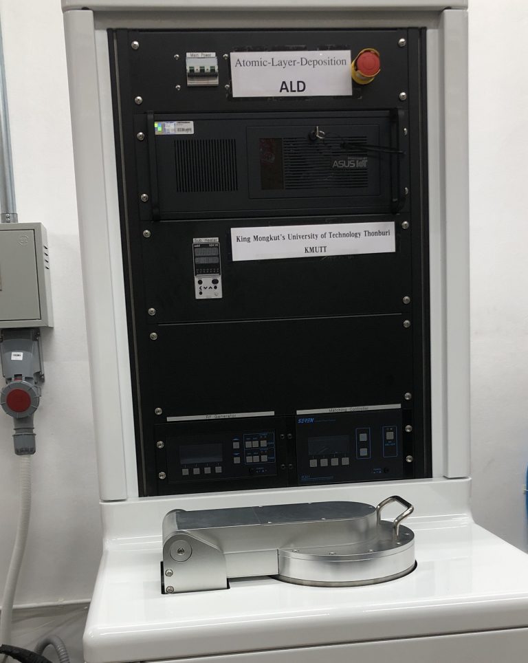
![]() 2nd floor of the Scientific Instrument Center for Standard and Industry Building King Mongkut’s University of Technology Thonburi (KMUTT) 126 Pracha Uthit Rd., Bang Mod, Thung Khru, Bangkok 10140, Thailand
2nd floor of the Scientific Instrument Center for Standard and Industry Building King Mongkut’s University of Technology Thonburi (KMUTT) 126 Pracha Uthit Rd., Bang Mod, Thung Khru, Bangkok 10140, Thailand
![]() +66 (2) 470 8803
+66 (2) 470 8803