Atomic Layer Deposition (ALD) is a thin film deposition technique that can be used for encapsulation in perovskite solar cells to improve their stability and performance. The process involves the sequential introduction of precursors that react with the surface of the material to form a thin film. The system includes RF-plasma up to 300W and four precursors available, for SnOx, Al2O3, TiO2 and ZnO.
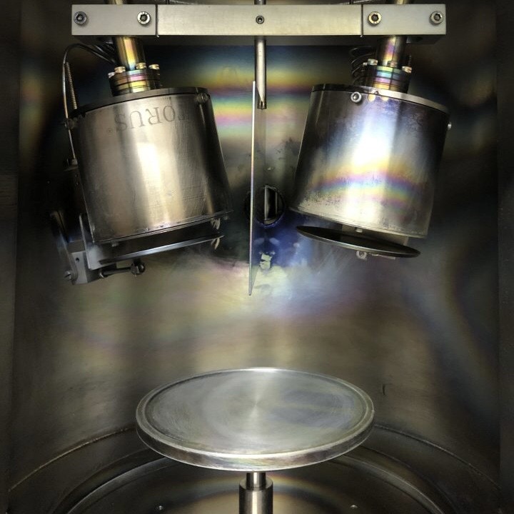
Dual-Chamber Thermal Evaportor
A dual-chamber thermal evaporator is a vacuum-based thin-film deposition system designed to deposit high-purity metal, semiconductor, and perovskite layers with minimal contamination. It contains two isolated deposition chambers, typically referred to as the source chamber (or “material chamber”) and the substrate chamber (or “main chamber”), connected by a high-vacuum transfer path. This configuration enables sequential layer deposition without exposure to air, which is crucial for air-sensitive perovskite and organic/inorganic semiconductors.
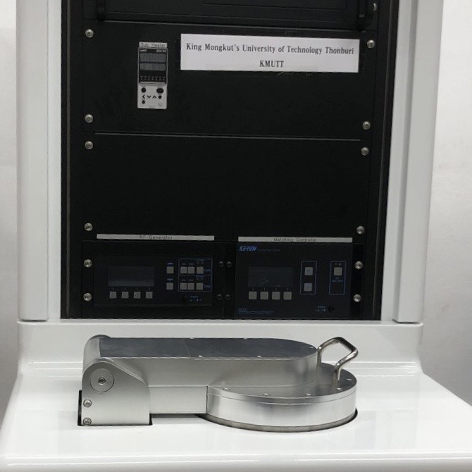
RF-DC sputtering system
Sputtering relies on a physical process where any particles of interest are ejected from a solid target material; this is due to the bombardment of the target by energetic gases. We use the RF&DC sputtering system for preparation of different layers of metal and semiconducting as well as composite materials. The advanced energy MDX 1.5K and RFX 600 equipped with ATX matching network are used as DC and RF power sources, respectively. A rotating substrate holder is installed in the system for uniformity of the deposited films.
Electron-Beam Deposition (E-beam)
E-beam (electron beam) deposition is a process used in the fabrication of thin films, including those for perovskite solar cells. For perovskite solar cells, materials like TiO2 or SnO2 or NiOx are commonly used for this purpose. The ETL/ HTL can be deposited using E-beam evaporation, ensuring a thin, uniform layer.
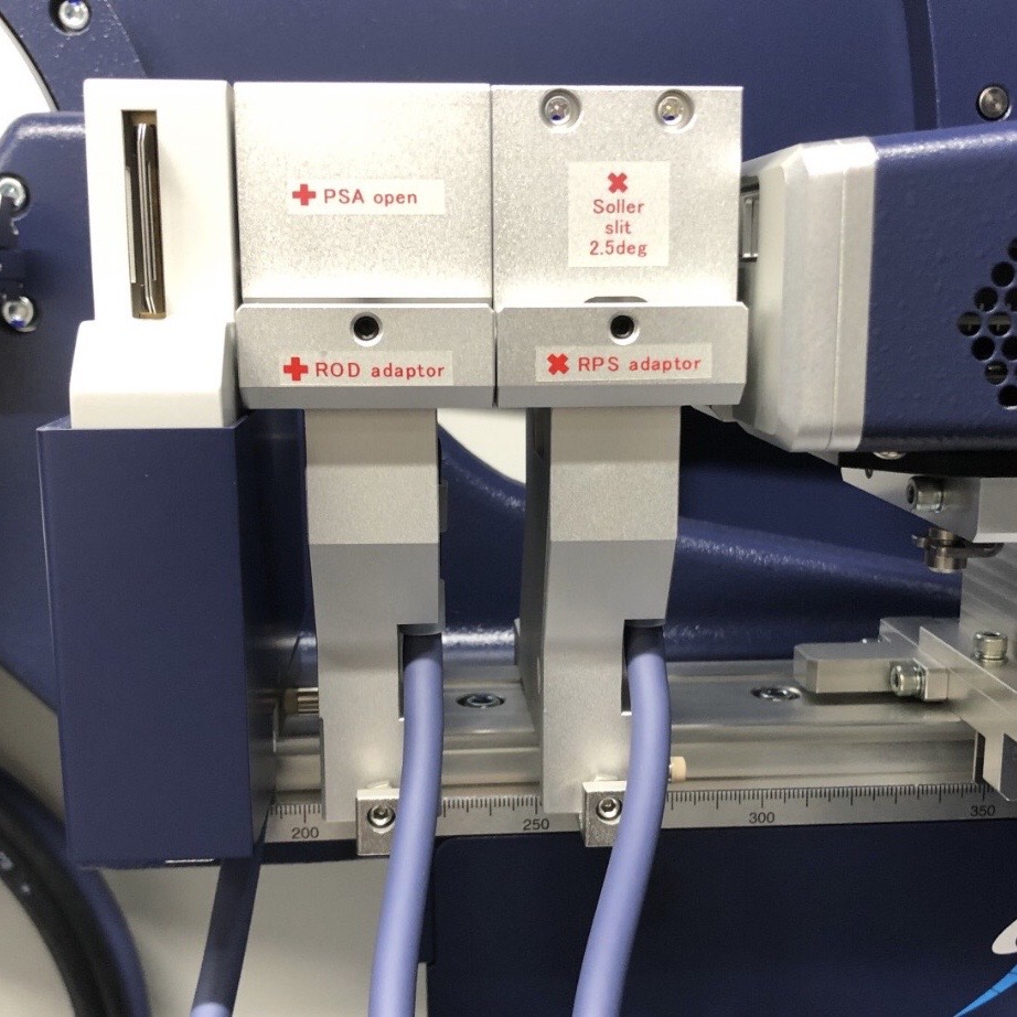
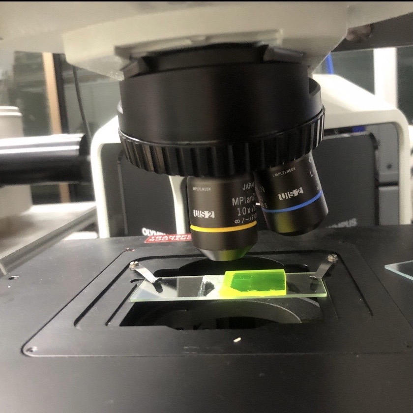
X-Ray Diffraction (XRD)
XRD is a fundamental tool in the analysis and understanding of crystalline materials. Its ability to provide detailed information about crystal structures and phases makes it invaluable in both research and industrial applications.
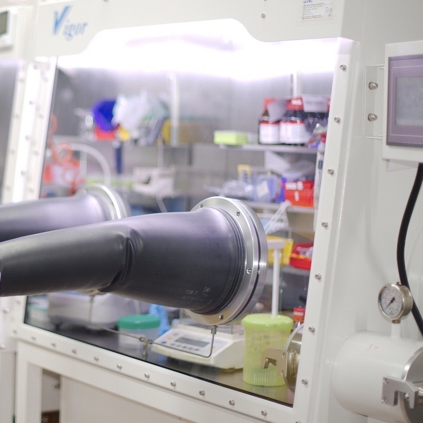
Nitrogen-Purged Glovebox
The use of a nitrogen-purged glove box is vital in the fabrication of perovskite solar cells due to the sensitive nature of the perovskite materials to environmental factors like moisture and oxygen. This controlled environment is key to achieving high-efficiency, stable, and reproducible solar cells.
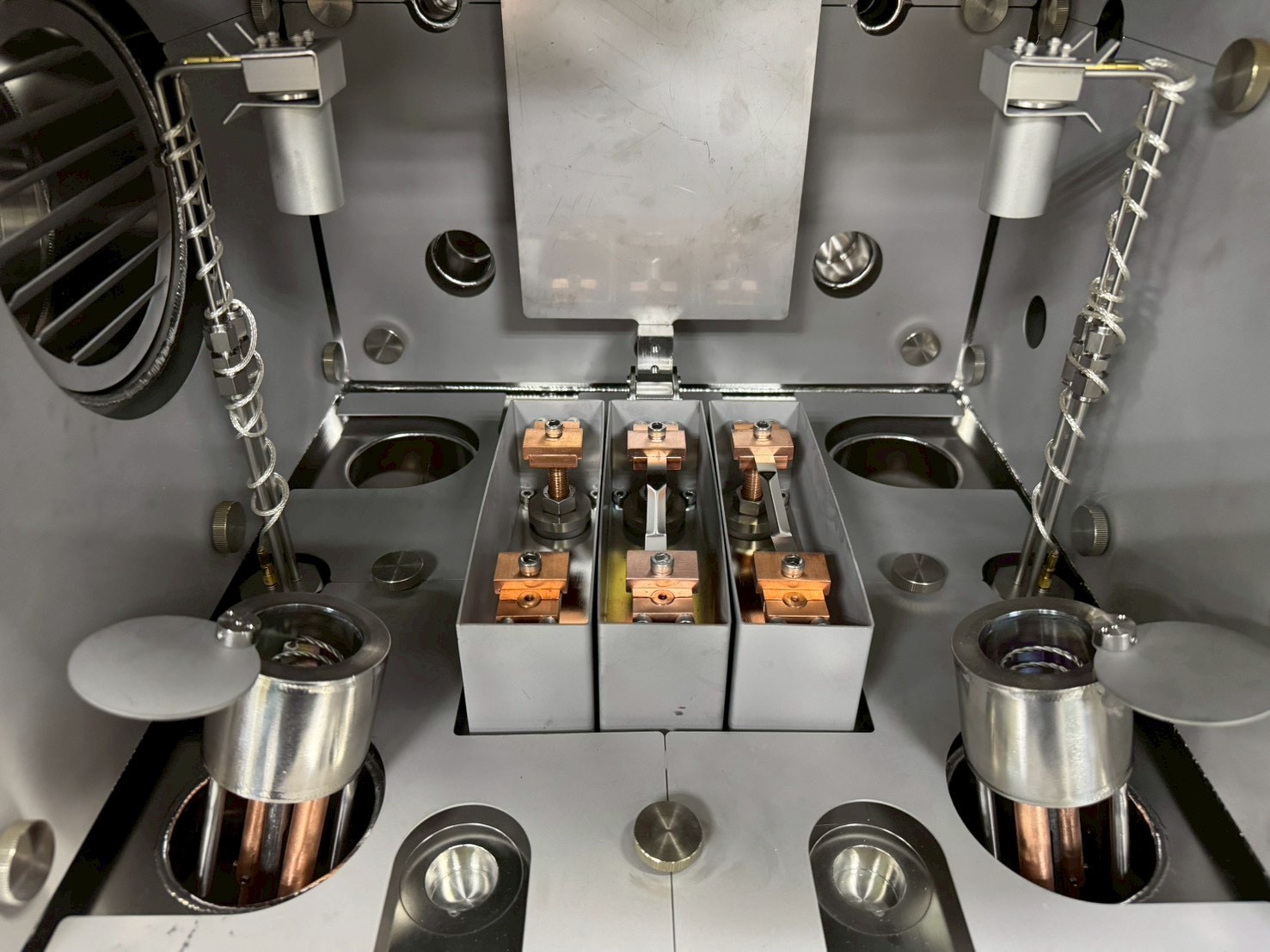
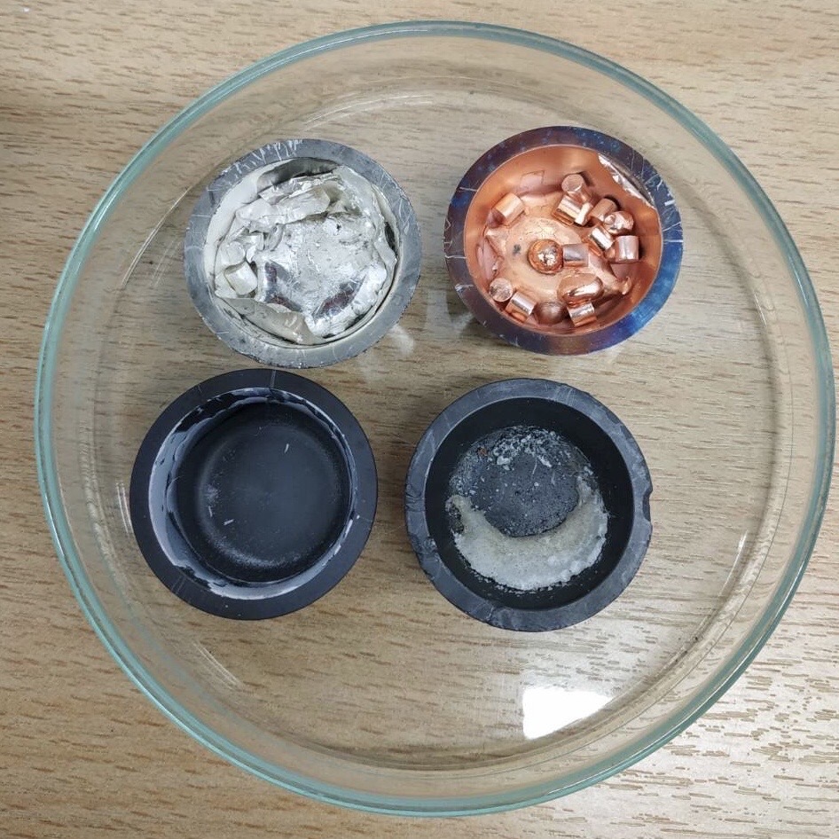
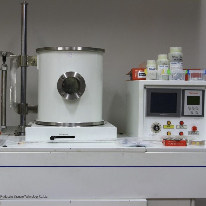
Thermal Evaporator
A thermal evaporator is a physical vapor deposition (PVD) system used to deposit high-purity metallic thin films—such as Au, Ag, Al, or Cr—onto substrates for micro-electronic devices. This deposition is driven by thermal (resistive) heating of the metal source in a high-vacuum environment.
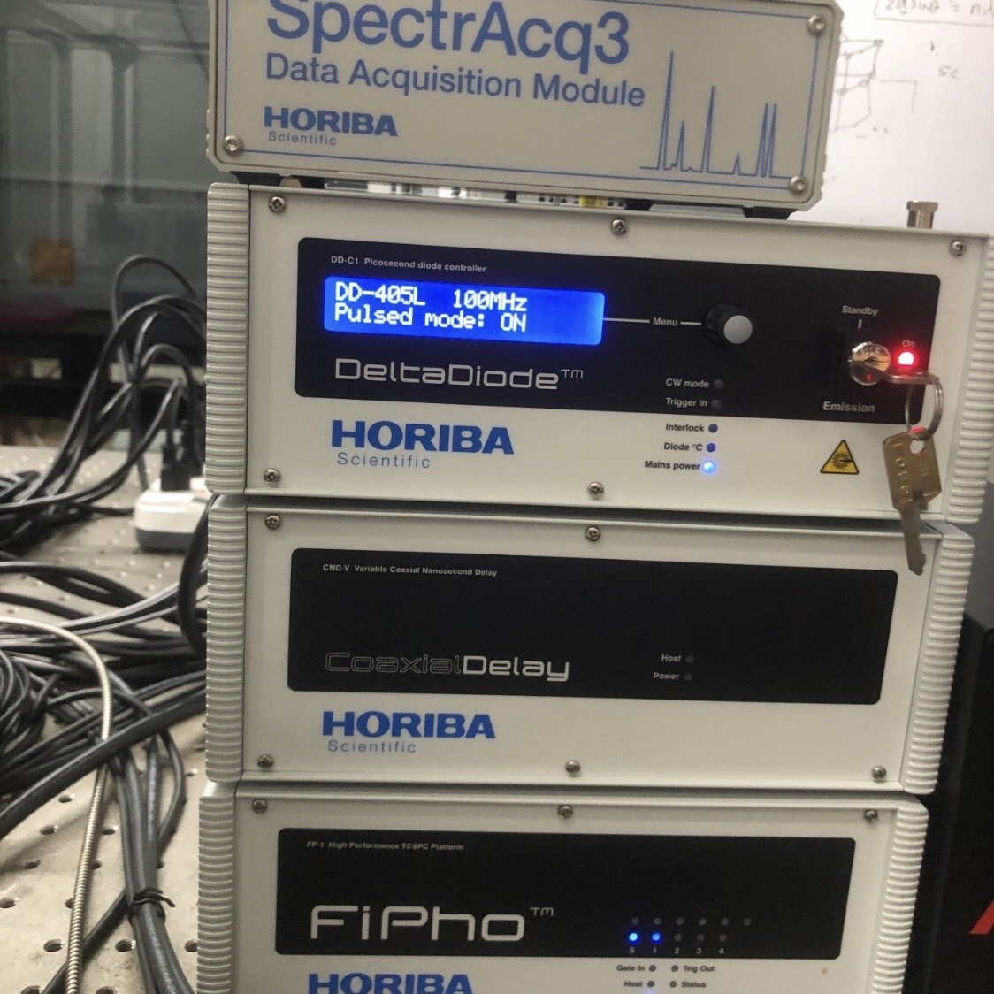
Time-resolved photoluminescence (TRPL)
The measurement of time -resolved photoluminescence (TRPL) is crucial in semiconductor and perovskite materials as it provides essential insights into the dynamics of charge carriers within perovskite materials. TRPL measurements reveal information about the behavior of charge carriers in perovskite materials, including their recombination rates and mechanisms.
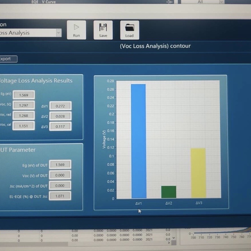
External Quantum Efficiency (EQE)
The External Quantum Efficiency (EQE) is an important parameter in the development of perovskite solar cells, as it provides critical insights into the efficiency and performance of these cells. EQE measures the fraction of incident photons that are converted into electrons, and it’s defined for each wavelength of the incident light.
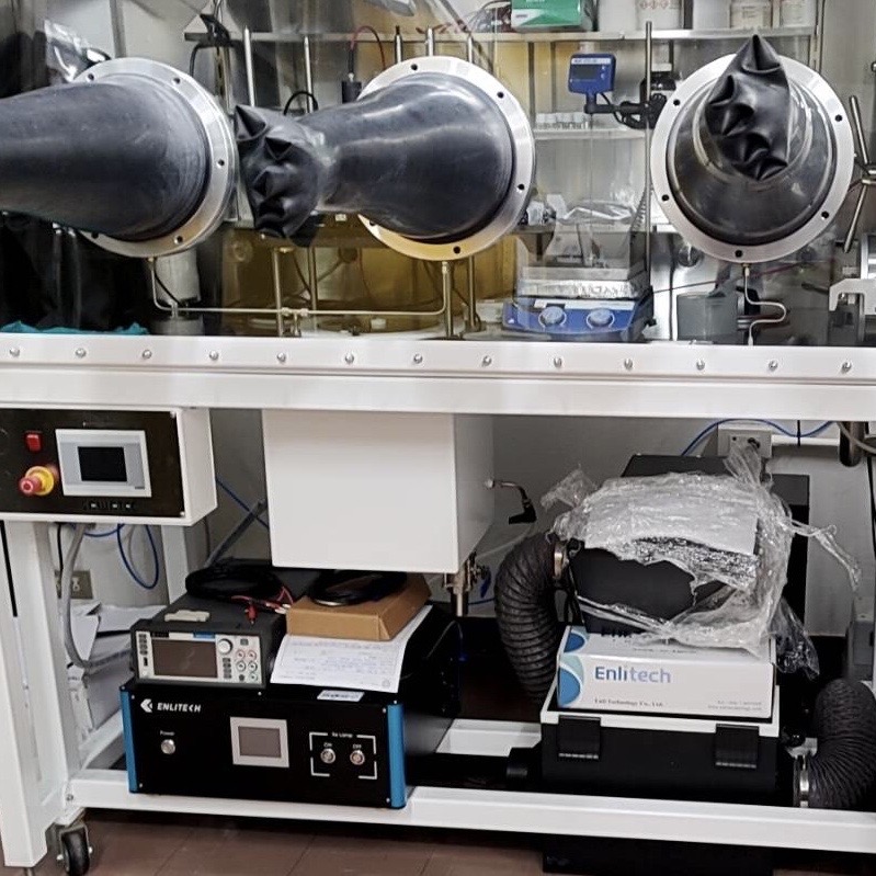
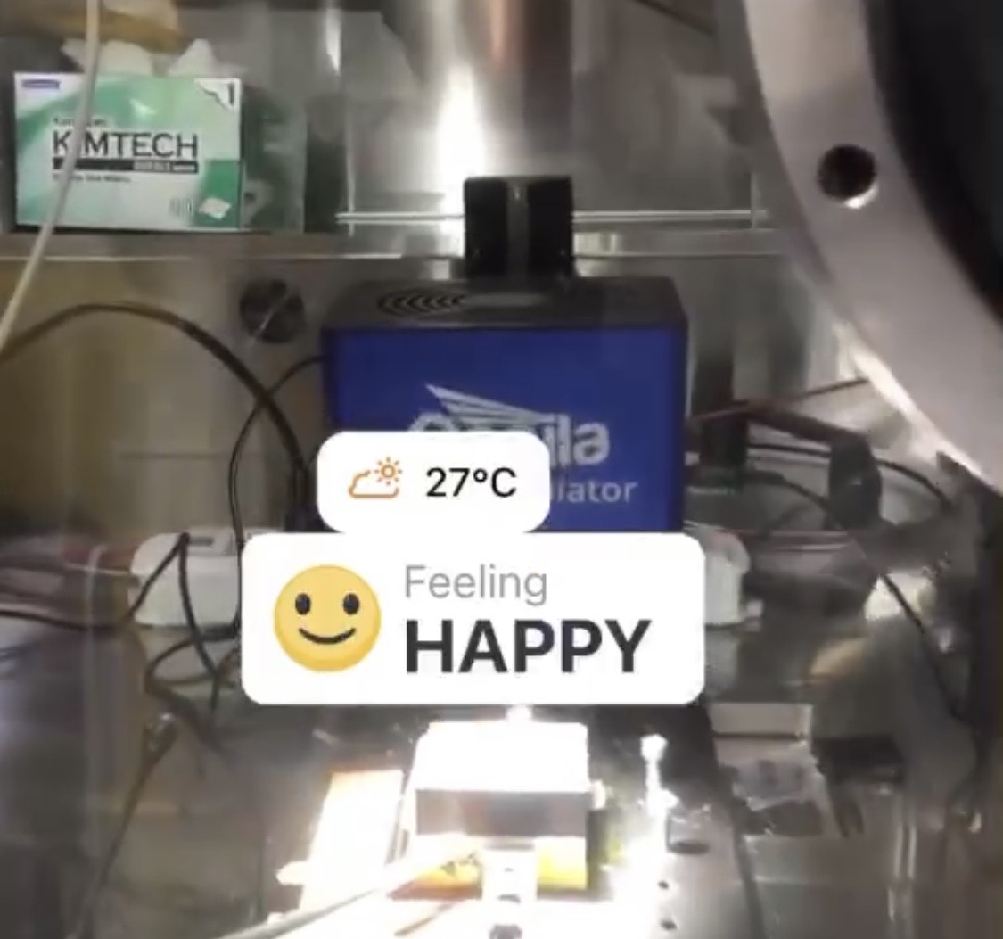
Sun Simulator
Solar simulators provide a standardized environment to test solar cells. They produce light with a spectrum and intensity that closely match those of the sun, ensuring that the performance of solar cells is measured under consistent and comparable conditions.
Low-Temp Electrical Measurement
Low-temperature electrical measurements are vital for a deeper understanding of the fundamental properties and behaviors of semiconductors. It provides insights into quantum phenomena, carrier dynamics, material defects, and device performance that are essential for the development and optimization of semiconductor technologies.
Photoluminescence (PL)
Photoluminescence (PL) measurement is a key technique in perovskite research due to its ability to provide valuable information about the optical and electronic properties of perovskite materials. PL is sensitive to defects, impurities, and non-radiative recombination sites within the perovskite material. These defects can act as traps for charge carriers, reducing the efficiency of solar cells. By studying the PL spectrum, we can identify and quantify these defects, guiding improvements in material synthesis and processing.
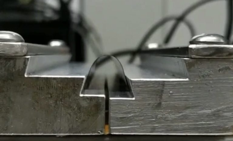
Mechanical Bending
The bending test is a critical evaluation method for flexible solar cells, as it assesses their mechanical robustness and durability under real-world conditions where bending and flexing are expected. Flexible solar cells are designed to be used in applications where traditional rigid solar panels are impractical, such as on curved surfaces, wearable electronics, or portable devices.
Stability test in a controlled environment
Stability testing of solar cells under a controlled environment is essential for isolating intrinsic degradation mechanisms from extrinsic environmental effects. By strictly regulating oxygen and moisture levels, our glovebox-based measurements enable accurate assessment of materials and interface stability, free from confounding degradation pathways such as moisture-induced perovskite decomposition, oxygen-assisted photo-oxidation, and electrode corrosion. This controlled setting is critical for perovskite solar cells, where ion migration, interfacial reactions and defect evolution can be strongly accelerated by ambient exposure.